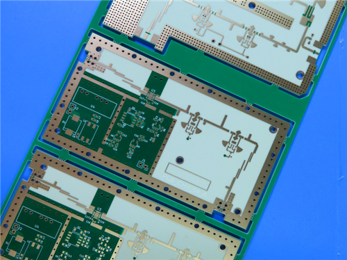
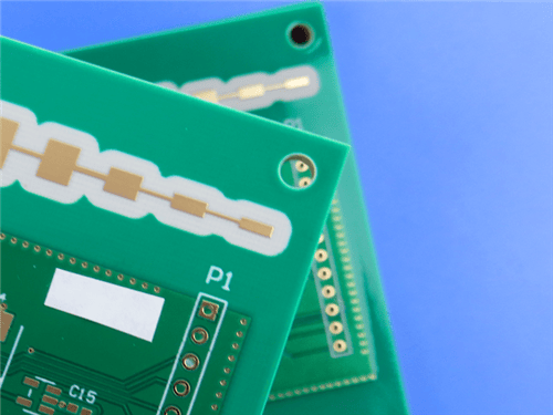
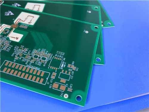
High Frequency 6-Layer Hybrid PCB RO4350B and S1000-2M with ENIG Finish
1.Introduction & Material Technology
RO4350B High-Frequency Material
Rogers RO4350B is a proprietary woven glass reinforced hydrocarbon/ceramic laminate offering:
Electrical performance approaching PTFE/woven glass
Standard epoxy/glass manufacturability
Cost-effective alternative to traditional microwave laminates
UL 94 V-0 rating for high-power RF designs
Key advantages:
Tight dielectric constant (Dk) control
Excellent dimensional stability (CTE matched to copper)
Reliable plated through-holes in thermal shock conditions
High Tg >280°C for stable processing
S1000-2M High-Performance Material
Complementary material providing:
Improved through-hole reliability with lower Z-axis CTE
Superior mechanical processability
Lead-free compatibility
Excellent anti-CAF performance
UV blocking/AOI compatibility
2.Key Material Properties
Key Material Properties(RO4350B)
Dielectric Constant of DK 3.48 +/-0.05 at 10GHz/23°C
Dissipation Factor of 0.0037 at 10GHz/23°C
Thermal Conductivity 0.69 W/m/°K
X axis CTE of 10 ppm/°C, Y CTE of 12 ppm/°C, Z CTE of 32 ppm/°C
High Tg value of >280 °C
Low water absorption of 0.06%
(S1000-2M)
Lower Z-Axis CTE for improved throughhole reliability
Excellent Mechanical Processability and Thermal Resistance
Leadfree Compatible
Tg180℃ (DSC), UV Blocking/AOI compatible
High heat resistance
Excellent Anti-CAF performance
Low water absorption
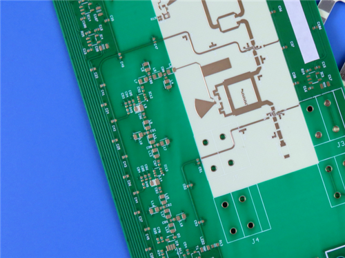
3.Complete PCB Specifications
Construction Details
| Parameter | Specification |
|---|
| Base Materials | RO4350B + S1000-2M |
| Layer Count | 6 layers |
| Dimensions | 76.5×83mm (±0.15mm) |
| Thickness | 1.5mm |
| Trace/Space | 4/4 mils |
| Hole Size | 0.3mm (min) |
| Via Types | Blind (L1-L2) |
| Copper Weight | 1oz (35µm) all layers |
| Via Plating | 20µm |
| Surface Finish | ENIG |
| Solder Mask | Blue (both sides) |
| Silkscreen | White (both sides) |
| Impedance Control | 50Ω (4mil top layer) |
| Electrical Test | 100% tested |
4.PCB Stackup: 6-layer rigid PCB
| Layer | Material/Type | Thickness | Dielectric Constant | Notes |
|---|
| L1 | Copper (Top Layer) | 35 μm | - | Signal layer, ENIG finish |
| RO4350B | 0.254 mm | 3.48 @ 10GHz | Core material |
| L2 | Copper (Inner Layer 1) | 35 μm | - | Power/Ground plane |
| Prepreg (1080 X2 RC63%) | 0.127 mm | 3.4 (typical) | Bonding layer |
| L3 | Copper (Inner Layer 2) | 35 μm | - | Signal layer |
| S1000-2M | 0.254 mm | 3.2 (typical) | Core material |
| L4 | Copper (Inner Layer 3) | 35 μm | - | Power/Ground plane |
| Prepreg (1080 X2 RC63%) | 0.127 mm | 3.4 (typical) | Bonding layer |
| L5 | Copper (Inner Layer 4) | 35 μm | - | Signal layer |
| RO4350B | 0.254 mm | 3.48 @ 10GHz | Core material |
| L6 | Copper (Bottom Layer) | 35 μm | - | Signal layer, ENIG finish |
5.Board Statistics
Components: 149
Total Pads: 215
Thru Hole Pads: 57
Top SMT Pads: 38
Bottom SMT Pads: 120
Vias: 79
Nets: 6
6.Manufacturing & Quality Standards
Artwork Format: Gerber RS-274-X
Quality Standard: IPC-Class 2
Via Types: Blind vias L1-L2
Availability: Worldwide shipping
7.Target Applications
Commercial airline broadband antennas
Microstrip and stripline circuits
Millimeter wave applications
Radar and guidance systems
Point-to-point digital radio antennas
High-frequency communication systems
8.Material Combination Benefits
The hybrid construction combines:
RO4350B's superior high-frequency performance
S1000-2M's mechanical reliability
Balanced CTE for dimensional stability
Cost-effective multilayer solution
|
.jpg)
